
We Asked Over 100 Engineers: why PCB Design Takes So Long? Here’s What We Found
Having talked to over 100 engineers in the past few months to gain a sense of what problems engineers face while designing PCBs, we found that engineering teams can take, on average, 2–3 months to get a PCB from concept to market-ready.
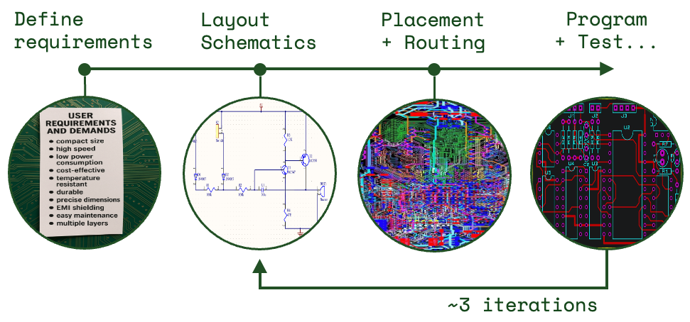
The team at siliXon have learned that the design flow can be broken down into four distinct stages:
1. Defining Requirements
With all good products, this starts off with knowing what exactly you will be building. What sort of inputs will it be expecting?
What will the output voltage be? What is the signal-to-noise ratio (SNR) of the device? Operating temperatures?
This stage takes a long time to define — and can take even longer if your customers don’t really know what they want themselves. In those cases, the engineer has to fill in the blanks.
2. Designing Schematics
Before designing your PCB, it’s best to come up with a blueprint of the circuitry, illustrating how every component connects to each other.
A clear schematic is critical, as any mistake here cascades through the rest of the design.
If a pin is wired incorrectly or an incorrect component is used and isn’t fixed, the entire design process may have to be restarted.
A popular tool for designing schematics is LTSpice. However, some engineers mentioned they actually prefer hand-drawing their designs due to the software being too slow for their workflows.
3. Placement and Routing
This is the crux of the design process. If the schematic lays out the blueprint, the placement and routing step allows that blueprint to become reality. Imagine the components on the PCB as puzzle pieces — engineers spend a lot of time deciding where each component goes, and how they’ll be connected via copper traces on the board.
This is also where collaboration tends to break down most often due to multiple engineers making edits, managing constraints, and running design rule checks (DRCs).
In our conversations with engineers, a recurring issue was component sourcing — having to compromise between price, functionality, and lead time. One engineer noted:
“It is a huge issue. If components [we need] go out of stock, we have to do some last-minute changes which could impact 30% of the project.”
Mistakes at this stage are expensive and often not caught until manufacturing, leading to wasted prototypes and weeks of delay.
4. Programming and Testing the Design
After the long process of choosing where components are placed and sending the design out for assembly, it’s time for testing.
The assembled PCB is tested under various conditions — temperature, noise, and other stress factors — to ensure it operates within the specifications defined by component datasheets.
At this stage:
- Microcontrollers are flashed with firmware by a separate team.
- Communication interfaces are verified.
- Each subsystem is tested to ensure it works as intended.
This phase takes a while because the design is passed between teams, and engineers told us it’s one of the most frustrating and time-consuming stages.
Common Pain Points
- Firmware bring-up pains: writing drivers, setting up communication protocols (SPI, I²C, UART), and debugging non-communicating peripherals.
- Hardware/software mismatches: pins assigned in the schematic don’t align with firmware assumptions.
- Testing bottlenecks: each design goes through power tests, functional verification, and sometimes compliance (EMC, safety) before it’s considered done.
Re-iteration due to bugs: with thousands of components, a single missed pull-up resistor can mean weeks lost waiting for a revised board.
What We Learned
From our conversations, it’s clear that the problem isn’t a lack of engineering skill — it’s the limiting tools that make the design process so long and tedious.
PCBs are inherently complex, so it’s natural that small mistakes occur during the process, leading to wasted electronics, money, and time.
At siliXon, we’re researching ways to integrate these workflows into a unified, feedback-driven environment — drastically reducing turnaround times from months to just a few hours, while maintaining design integrity and manufacturability.